INFINEON SETS A NEW MILESTONE IN GAN TECHNOLOGY

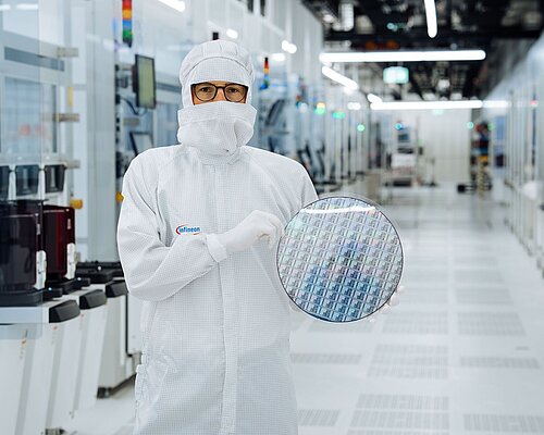
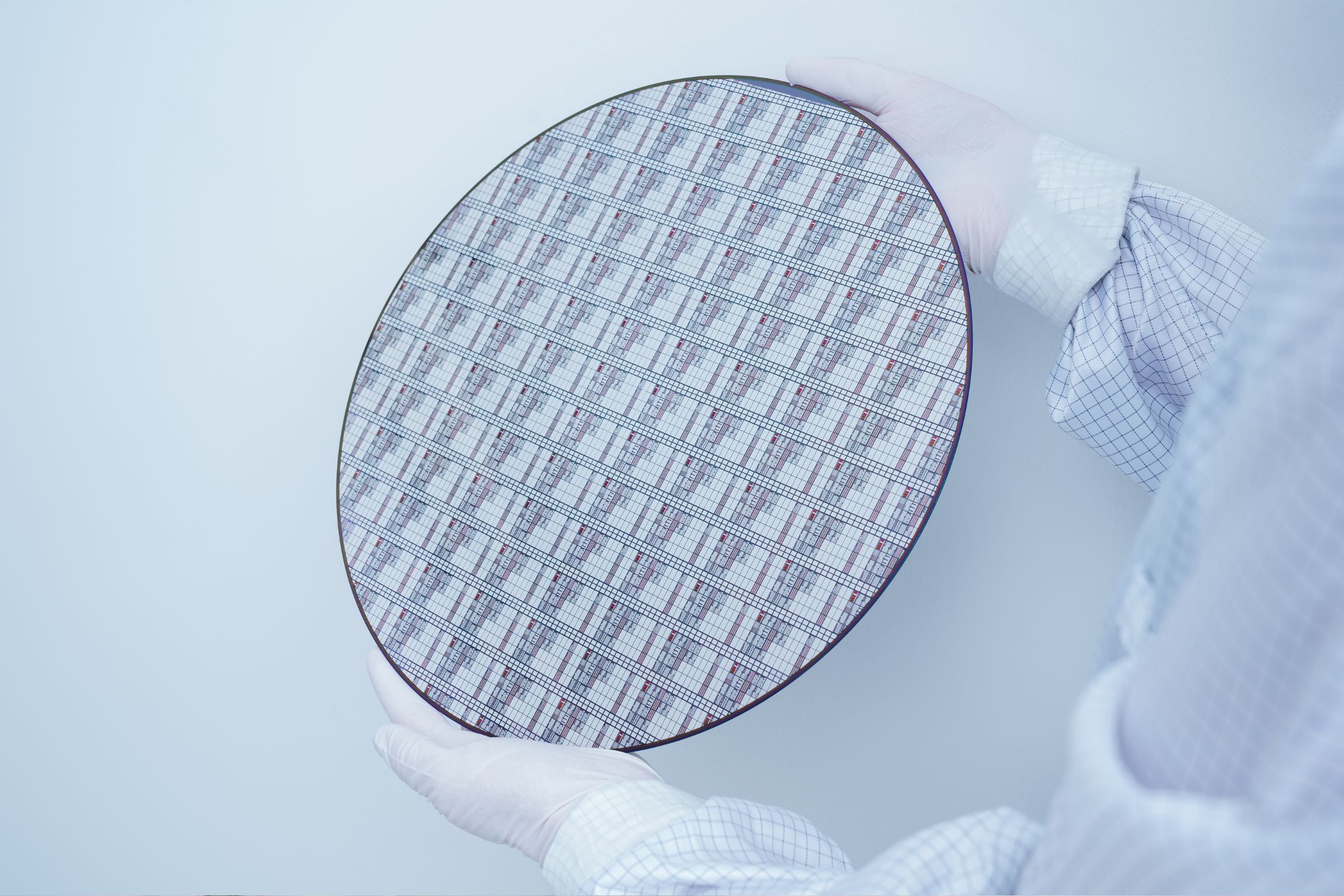
Infineon Technologies AG has succeeded in developing the world's first 300 millimeter gallium nitride (GaN) wafer technology for power electronics at its Villach location. This breakthrough innovation will not only revolutionize the GaN industry, but also significantly increase production efficiency and enable more cost-effective manufacturing.
VILLACH AS AN INNOVATION CENTER
The Villach location plays a central role in the development of this innovative technology. Here, in the Power Fab, the production of the new wafers was successful. 300-millimeter GaN production will be integrated into existing production lines, enabling rapid market access and efficient capital deployment. This strategic decision will help Infineon take a leading role in the growing GaN market, which is expected to be worth billions of dollars by the end of the decade.
ADVANTAGES OF 300 MILLIMETER GAN TECHNOLOGY
The switch to 300 millimeter wafers brings significant advantages. Compared to conventional 200 millimeter wafers, 2.3 times more chips can be produced per wafer. This leads not only to increased production efficiency, but also to a reduction in size, weight and cost of the final products. Thanks to the existing 300 mm silicon high-volume manufacturing, Infineon can further reduce the costs of GaN production. In the long term, the aim is to bring the cost of GaN to the level of silicon.

VERSATILE APPLICATIONS
The new GaN semiconductor technology offers a wide range of possible applications in the areas of industry, automotive and consumer electronics. Examples range from power supply for AI systems to solar inverters to chargers and motor control systems. The advanced manufacturing technology not only improves performance, but also ensures stable supply for customers worldwide.
LOOKING INTO THE FUTURE
Infineon's breakthrough marks a significant step in the semiconductor industry. The company plans to further expand its GaN capabilities to meet increasing demand. The official presentation of the new 300 millimeter GaN technology will take place at electronica in November 2024 in Munich.
With this technological milestone, Infineon is once again setting a strong example in the global semiconductor industry and is driving development towards an energy-efficient, digital future.
FACTS & FIGURES (2024):
- Location:
- Headquarters: Villach
- Branches: Graz, Klagenfurt, Linz, Innsbruck and Vienna
- 5,886 employees from 79 nations
- around 2,500 of them in research and development
- 5.6 billion euros in sales in the 2023 financial year
- 672 million euros in research expenditure